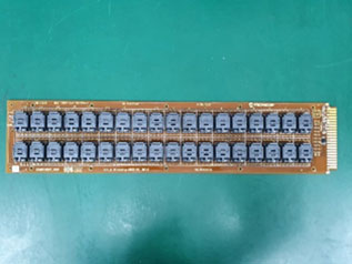
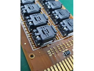
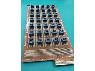
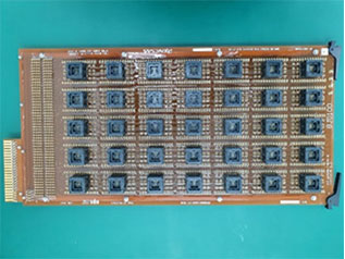
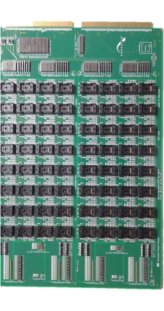
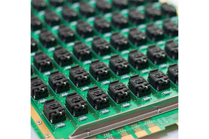
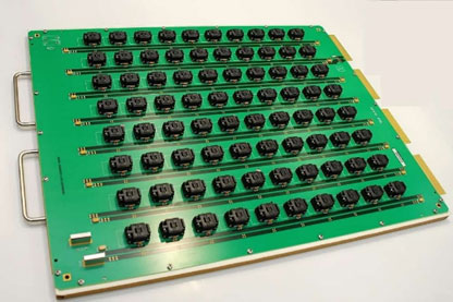
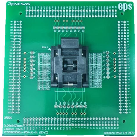
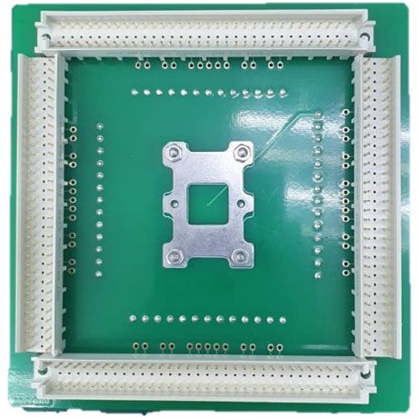
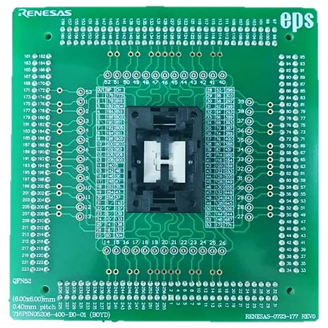
BURN IN BOARD DESIGN
Embedded Product Solution (EPS) designs and manufactures burn-in boards for use during burn-in and testing of a wide variety of electronic devices for many different types of burn-in systems. Each burn-in board is designed by engineers specializing in burn-in board design and can be formulated to meet the customer’s specific application requirements and specifications.
We can design and build burn-in boards for your requirements as well as custom burn-in chambers.
Our experienced PCB burn-in board designers are ready to work with you on the details of your requirements and, where needed, provide advice regarding best practices for issues such as laminate choice, space, and trace requirements, and other needs.
- Dedicated and universal board designs
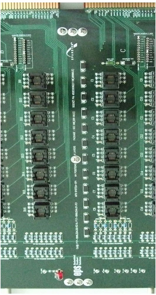
- Gold-plated connectors and socket lands
- All burn-in board styles available
- Loader/unloader compatibility
- Suitable to be used in hast environment
- Leakage or shorting in hast environment is prevented by a layer of conformal coating
- High temperature board materials are used to prolong the life span of the board
- 4 – 16 layers design
- Suitable to be used in high or ambient temperature environment
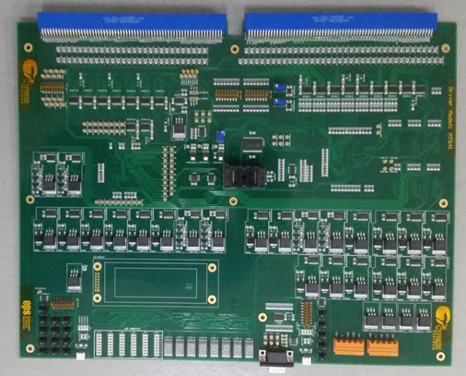
- Real time monitoring burn-in
- Signal trace impedance is controlled typically at 50Ω and 75Ω
- 6 – 16 layers design
- Signal termination and daisy chain routing are designed to maintain signal integrity
- Board materials are used to prolong the life span of the board
- Suitable to be used in high temperature environment
- Dynamic burn-in where signals are pumped in to stress the DUT
- 6 – 16 layers design
- Signal trace impedance is controlled typically at 50Ω
- High temperature board materials are used to prolong the life span of the board
Our ESD Board compatible with MK1 to MK4 ESD Tester
- Logic Sequencer address generator
- Customize pattern address generator
- Able to support address from A0 to A38
- 0.5A Output pulse current per channel
- Suitable to be used as memory device burn in driver board

Specifications of the burn in board design
| Specifications | HAST BIB | HTOL BIB | Cycling Board | ESD Test Board | Others |
|---|---|---|---|---|---|
| No. of Layers | 4 - 8 | 6 - 10 | 6 - 12 | 2 - 6 | 1 - 16 |
| Board Material | BT-Resin Nelco 4000 Polymide |
BT-Resin Nelco 4000 Polymide |
BT-Resin Nelco 4000 Polymide |
FR4 BT-Resin |
FR4 BT-Resin Polymide |
| Board Thickness | 0.06" | 0.06" | 0.06" | 0.08" | 0.01" - 0.26" |
| Board Thickness Tolerance | ±10% | ±10% | ±10% | ±10% | ±5%/ ±10% |
| Minimum Outer Line Width | 4 mil | 4 mil | 4 mil | 4 mil | 4 mil |
| Minimum Inner Line Width | 3.5 mil | 3.5 mil | 3.5 mil | 3.5 mil | 3.5 mil |
| Minimum Outer Space, Trace/ Trace | 4 mil | 4 mil | 4 mil | 4 mil | 4 mil |
| Minimum Inner Space, Trace/ Trace | 4 mil | 4 mil | 4 mil | 4 mil | 4 mil |
| Minimum Space, PCB Edge to Conductor | 8 mil | 8 mil | 8 mil | 8 mil | 8 mil |
| Layer-to-Layer Registration | 6 mil | 6 mil | 6 mil | 6 mil | 6 mil |
| Minimum Component Pitch | 0.02" | 0.02" | 0.02" | 0.02" | 0.02" |
| Minimum Hole Size | 6 mil | 6 mil | 6 mil | 6 mil | 6 mil |
| Final Finishing | Immersion Gold Hard Gold |
Immersion Gold Hard Gold |
Immersion Gold Hard Gold |
Immersion Gold Hard Gold |
HASL Immersion Gold Hard Gold OSP |
| Silk Screen | White Gold |
White Gold |
White Gold |
White Gold |
White Gold |
| Operating Temperature | 150°C | 150°C | 150°C | 150°C | 125°C - 150°C |